
I was recently asked what equipment is necessary to set up a new AFM lab, so here goes:
Materials necessary to set up a new AFM lab
Note: Many manufacturers include a lot of these items when you buy an instrument; check before ordering. I have only included estimated prices for items with high cost.
Mandatory Items
1. Calibration/certification product. Usually a silicon grid with repeating features. See extensive list of suppliers here:
SPM References and Standards
Note: This is the most expensive item, but absolutely necessary. The importance of calibration is discussed in my book (especially Appendices A and B). Take care of your calibration artifact once you have it.
Estimated cost: 300-1000 dollars, depending on model and supplier. Traceable standards will be more expensive.
2. Cantilevers / Probes. Of course these are necessary for all work. You typically get a few with a system, and can also beg samples from manufacturers, but you will need more, and soon! See extensive list of suppliers here:
Where to buy : SPM Probes
Estimated cost: 300 dollars for a box of 20
3. Anti-vibration solution. There are many different types of vibration-damping equipment, see chapter 2 of my book. They can usually be bought with instruments, but at additional cost. Suitable vibration / acoustic isolation stages for AFM instruments can cost from 2,000 to 10,000 dollars.
4. Tweezers. These are important for handling samples, and handling probes. I recommend two types, specific AFM probe-handling levers with specially shaped ends, and type 2A (flat, rounded ends, preferably non-magnetic), for handling samples and sample mounting discs.
I often buy from Ted Pella, see here for probe tweezers, and here for type 2A, but most microscopy suppliers carry these, or some equivalent. Note: on a budget, type 2A also can be used for probes, but I highly recommend that you keep a clean pair of tweezers, especially for handling probes.
5. Sample mounting discs. These are simply magnetic steel discs of about 10-15 mm diameter, and 1 mm thick. You can even make them yourself. Most microscopy suppliers sell them in tubes of 50-100. See here for the ones at Ted Pella.
6. Sample mounting adhesive tabs. To stick your sample onto the metal discs (above). See here for example at SPI. Alternatively, can be easily replaced with double sided sticky tape with few problems.
Optional Items
7. A source of very clean water. Some labs use milliQ water, and this is fine for most work, but you can also find ultra-pure bottled water, which I mostly use. See chapter 4 of my book.
8. A source of clean gas. Used for removing dust from samples. At a pinch you can use a “blower”, like this: Rocket Air Blaster.
9. Adhesive for when double-sided sticky tape is not enough: 2 part epoxy is the gold standard, superglue (cyanoacrylate) can also be used, but not for work in liquids.
10. Solvents for cleaning, etc.
11. Optical microscope and / or magnifier. Usually AFMs have an integrated optical scope, that can be used to obtain optical images of the sample. Depending on your application, and how good the attached scope is, you may want a separate optical microscope to view samples before putting them in the microscope and possibly to record good optical images. This can help greatly with sample preparation. It is also VERY useful to have a magnifier or small microscope to help with probe seating, i.e. to make sure your probe chip still has a cantilever and that you have placed it in the probe holder of the AFM correctly.
12. Other susbstrates. Depending n the kind of work you need to do, you will want substrates to deposit your samples on. These might be optical glass slides, coverslips, mica, or HOPG. flat silicon samples can also be useful. Most AFMs work with 1cm diameter samples or smaller.
Instrument Building / Repair / Diagnostics
For this, you’ll also want many small tools, including Allen (hex) keys, screwdrivers, etc. Glue, including superglue. Multimeter. Good soldering iron and solder, preferably silver solder with a flux core.
Room Requirements
For the room you are going to put the AFM in, there are not many real “must-haves”. But it’s recommended you use a small lab, with little foot traffic, or at least one where the people can be expected to keep quiet. Basement labs are preferred to upper stories. These are all due to vibration and acoustic noise issues. It’s useful to have air-conditioning, especially if you expect to have large temperature variations during the day. But you must be able to turn this off in case it interferes with high-resolution work.
As always, suggestions and additions to this are welcome - go HERE for the contact form.
Copyright Peter Eaton 2012-2018
- Details
- Hits: 25135
Every year in our AFM training course, we hold a little competition among the students to produce and process an AFM image. The prize is always a liquid product from the city of Porto!
This year, the overall prize was won by this nice treatment of human red blood cells sent in by Akmaral.
|
||
Thanks to Christie for donating the blood!
In addition, this year, we have a special prize for “outstanding image processing”, which goes to Tobias for this unusual image presentation: I can only show you a photo of the image, as he 3D-printed the AFM image of 90nm nanoparticles. Great one, Tobias!
3D printed image of Nanoparticles from Tobias Burger |
||

Congratulations to Akmaral and Tobias, your prizes and certificates will be with you soon!
Thanks to everyone who entered the competition this year. Hope to see you again!
- Details
- Hits: 4114
One of the most important components of an AFM is the probe. AFM probes are made of a chip or substrate, a cantilever, and a tip. Usually, these are manufactured in one piece of silicon (or silicon nitride, Si3N4), by MEMS manufacturing techniques. In this way a wafer (with 400 or more probes) is manufactured at one time, with reasonable reproducibility of probe characteristics across the probes.
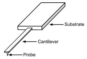
Design of typical AFM probe, showing the substrate, cantilever and tip (probe).
Importantly, nearly all probes are interchangeable, so it’s possible to use probes from different manufacturers in your instrument. Thus, there is a fairly competitive market in AFM probes, and you can find a variety of probes from value to high-cost offerings, and an enormous range of probes, with different coatings, and physical properties, suitable for a wide range of applications. There are so many different probes here, that it’s not worth listing them all, so this page just links to the manufacturers of probes that I know of. Some companies resell probes from other manufacturers,such distributors are listed on this page. But here I list only the manufacturers. The manufacturers are listed in no particular order.
AFM Probe Manufacturers
|
Bruker |
Bruker (until recently Veeco) manufacture a huge range of probes, as well as reselling probes from various other producers. They have many representatives, as well as selling direct in the U.S. |
|
Applied NanoStructures |
AppNano manufacture a wide range of standard and speciality probes- they are resold by various companies, and also sell direct |
|
Nanoworld |
Nanoworld manufacture a very large range of standard and speciality probes - resold by various companies. Also branded as nanosensors |
|
Mikromasch |
Mikromasch manufacture a very wide range of probes, both standard and speciality. They sell direct and are re-sold |
|
NT-MDT www.ntmdt-tips.com |
NT-MDT manufacture many standard and specialty probes, including with a wide range of coatings |
|
Olympus |
Olympus manufacture many “standard” and novel probes, including the biolever-often used for force spectroscopy. They do not sell their own probes, but they are sold by a large number of companies |
|
Artech Carbon |
Artech Carbon make single-crystal diamond porbes, which are very sharp and wear-resistant. |
|
Team Nanotec |
Team Nanotec make a variety of specialist AFM probes, including metrology tips, high-aspect ratio probes, MFM probes, etc. They both sell direct and are re-sold |
|
Asylum Research |
Asylum make various speciality probes of their own design, as well as reselling various other brands. Asylum are now part of Oxford Instruments |
|
Micro2Nano www.micro2nano.com |
Korean company, Micro2Nano manufacture tetra brand probes which are resold, and offer a custom probe service |
|
Budget Sensors budgetsensors.com |
Budget Sensors manufacture a wide range of probes, including mix-and-match boxes. They have an online shop, and are resold |
|
sQube |
sQube manufacture a range of colloidal probe cantilevers, check their webpage for link to distributor |
|
Kelvin Nanotechnologies www.kelvinnanotechnology.com |
Based on the campus of Glasgow University, Kelvin Nanotechnologies manufacture scanning thermal probes |
|
NaugaNeedles |
Nauganeedles produce specialised probes with semiconductor nanowires grown from the end, useful for metrology and electrical applications |
|
NuNano |
Nunano is a Bristol (UK)-based startup specialising in SPM probe manufacture. Offer custom probe design. |
|
Carbon Design Innovations |
CDI manufacture AFM probes modified with carbon nanotubes on the tip |
|
Smart Tip www.smarttip.nl |
Based in the Netherlands, Smart Tip make specialised probes, such as magnetic MFM probes |
|
Novascan |
Company that specialises in colloid probes and chemically modified probes |
|
SCL-Sensor Tech. |
Company that specialises in self-sensing and self-actuating probes |
Once again, distributors can be found here.
If I any have missed any manufacturers ,or made any other errors, please feel free to make suggestions, via the contact page.
- Details
- Hits: 50801
Atomic Force Microscopy (AFM) is a high resolution technique to measure the topography of samples. However, in order for such measurements to be accurate, the AFM must be calibrated, so that the results can be trusted. The commercial materials listed here are suitable for making such calibrations of AFM instruments.
This information on AFM standards is extracted from my forthcoming book "Atomic Force Microscopy".
Please get in touch if any information is inaccurate or you know of another standard or supplier.
See appendix B of Atomic Force Microscopy for calibration procedures.
X-Y Standards
These are standards to calibrate or check linearity in the X-Y axis in SPMs.
|
Source |
Standard |
|
VLSI standards |
many in µm range (silicon, 2D) 100 to 1000 nm (silicon, 1D) |
|
Ted Pella |
144 nm (aluminium on Silicon) 300 nm (titanium on silicon) |
|
MikroMasch |
3 and 10 µm, HOPG |
|
SPI Supplies |
300 or 700 nm (metal-coated silicon) |
|
Electron Microscopy Sciences |
300 or 700 nm (metal-coated silicon) |
|
Applied NanoStructures |
Various in micrometer range (metal-coated silicon). I personally tried use these standards. |
|
Bruker |
1, 2, 10, 15 µm (silicon) |
|
NT-MDT |
278 nm (aluminium on glass, 1D) 3 µm (silicon, 2D) |
|
Asylum Research |
10 and 20 µm pitch (metal on silicon) |
|
Nanosensors |
100, 200 or 300 nm (silicon) 4, 8 and 16 µm (silicon |
|
BudgetSensors |
500 nm, 5 and 10 µm - SiO2 on silicon. |
|
Team Nanotech |
Pitch and feature width standards |
|
Geller Micro |
Geller sell references and standards (including traceable ones), suitable for AFM as well as EM. |
Z standards
Here are standards to calibrate the z scale. Sometimes these can be the same ones as used for the x-y axis calibration, but often they are separate samples.
|
Source |
Z calibration standard |
|
VLSI standards |
various silicon and quartz |
|
MikroMasch |
Various in silicon, HOPG |
|
NTT AT |
Silicon monatomic steps (0.31 nm) |
|
Ted Pella |
20, 100 and 500nm (Silicon) |
|
Applied NanoStructures |
10nm, 1µm |
|
BudgetSensors |
10, 100 and 500 nm steps - SiO2 on silicon |
|
Veeco |
2, 100, or 200 nm (silicon) |
|
NT-MDT |
Various steps in silicon and atomic steps in Silicon (0.31 nm) |
|
Asylum Research |
200 nm (metal on silicon) |
|
Nanosensors |
8nm (silicon) |
|
Silios Technologies |
2, 5 and 10 nm (silicon) 1 nm "in development" |
Other standard materials include ultraflat samples - mica and HOPG, available from various suppliers, and quartz ultraflat sample from nanosensors.
Particle Standards
Particle samples are also useful both to calibrate the tip and as height references.
|
Supplier |
Particle sample |
|
Tedpella |
Gold colloids in 5, 15, or 15 nm diameter |
|
Edmund Optics |
Polystyrene nanospheres in a range from 20 to 900 nm |
|
Evident Technology |
Quantum dots ranging from 2.2 to 5.8 nm |
|
Electron Microscopy Sciences |
Colliodal gold in 0.8 to 25 nm diameter |
LFM Standards
Samples for calibrating LFM , with fixed angle slopes are:
|
Supplier |
LFM sample |
|
Mikromasch |
Triangles (silicon), top angle 70 ° Steps with sloped edges (silicon), slopes 54 ° |
|
Edmund Optics |
Ruled diffraction gratings, with various angles |
Phase References
Samples for calibrating phase are available from Asylum Research and EMS. Both are polymer samples with regions of different hardness.
Probe Shape Calibration Samples
These are samples you can image with the AFM in order to get an in situ measurement of the radius and shape of the probe tip.
|
Supplier |
Sample |
|
Aurora NanoDevices |
Tip check sample (100 nm z-scale). Nioprobe tipcheck sample ( 10 nm z scale) |
|
Mikromasch |
Porous aluminium |
|
NT-MDT |
Silicon spikes |
|
BudgetSensors |
Thin film on silicon wafer, with sharp pyramidal spikes. I have used this sample, and it can be used in contact or oscillating modes to characterise probe tip shape. |
Feel free to get in touch with any updates / corrections.
- Details
- Hits: 42181
This page has a list of corrections to the book "Atomic Force Microscopy". If you notice any more mistakes, please let me know here. That way I can correct them in the next edition!
Important Note: All these errors will be corrected in the upcoming paperback edition. If you know of any more, let me know!
Errors
- Page 30 - Equation 2.6: Verr is used in place of Zerr in the first term.
- Page 38 - The last paragraph erroneously refers to equations 2.5, 2.6 and 2.7, where it should be 2.7, 2.8 and 2.9, respectively.
- page 53 - referring to the figure shown below:
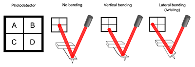
In this figure, vertical bending is detected as "(A+B)-(C+D)", i.e. the difference of the top two and bottom two segments. On page 53 the book erroneously says "(A+B)-(C-D)".
- Page 56 - Figure 3.6 Should read: "B-intermittent contact oscillation (large)".
- Page 66 - Legend refers to colours in the image where there are none.
- Page 114 - Section 5.2.4: Three-dimensional views. Should read: "...special glasses to differentiate the left eye's and right eye's views...".
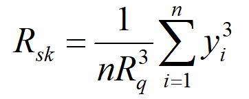
- Page 116 - Table 5.2. The Formula for skewness is incorect. The exponents should be 3, not 4. i.e., as shown below
- Page 164 - Misspelling of "fimbriae" as "fibriae".
Thanks very much to everyone who informed me of these errors!
- Details
- Hits: 12386
Subcategories
Page 6 of 21